One integrated facility for PCB fabrication, assembly, sourcing and testing. Our engineering team reviews every file before production starts.
1–32 layers, HDI, rigid-flex, high-frequency materials.
01005–BGA, mixed technology, 10 SMT lines.
Global distributors, genuine parts, flexible quantities.
From Gerber & BOM to tested, ready-to-ship boards.
24h prototypes and smooth scale-up to volume.
AOI, X-Ray, ICT, FCT plus full system assembly.

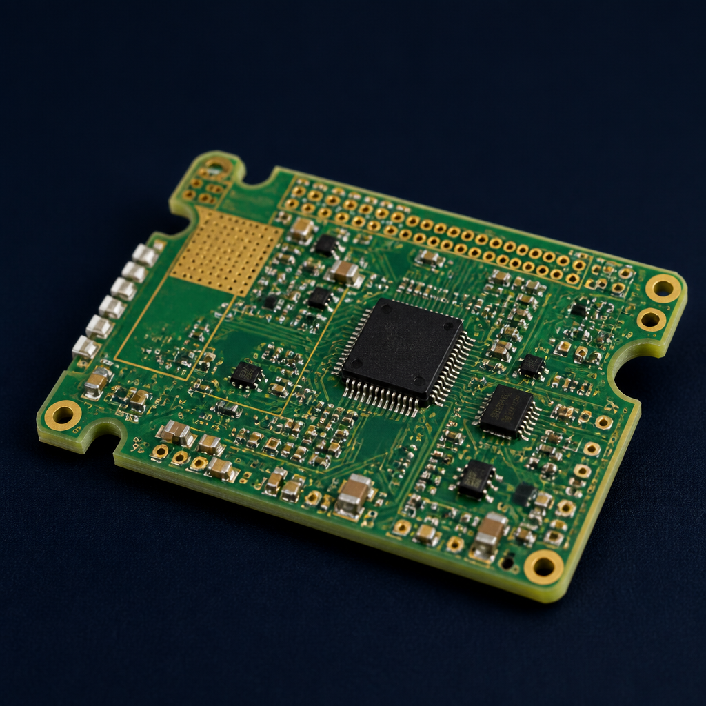
Our factory fabricates advanced boards for every application — from simple 2-layer boards to complex 32-layer HDI and rigid-flex stacks.
| Layer Count | 1 – 32 layers |
| Min. Trace / Space | 3 / 3 mil |
| Min. Drill Hole | 0.15 mm |
| Max. Board Size | 610 × 610 mm |
| Board Thickness | 0.2 – 6.0 mm |
| Impedance Tolerance | ±5% |
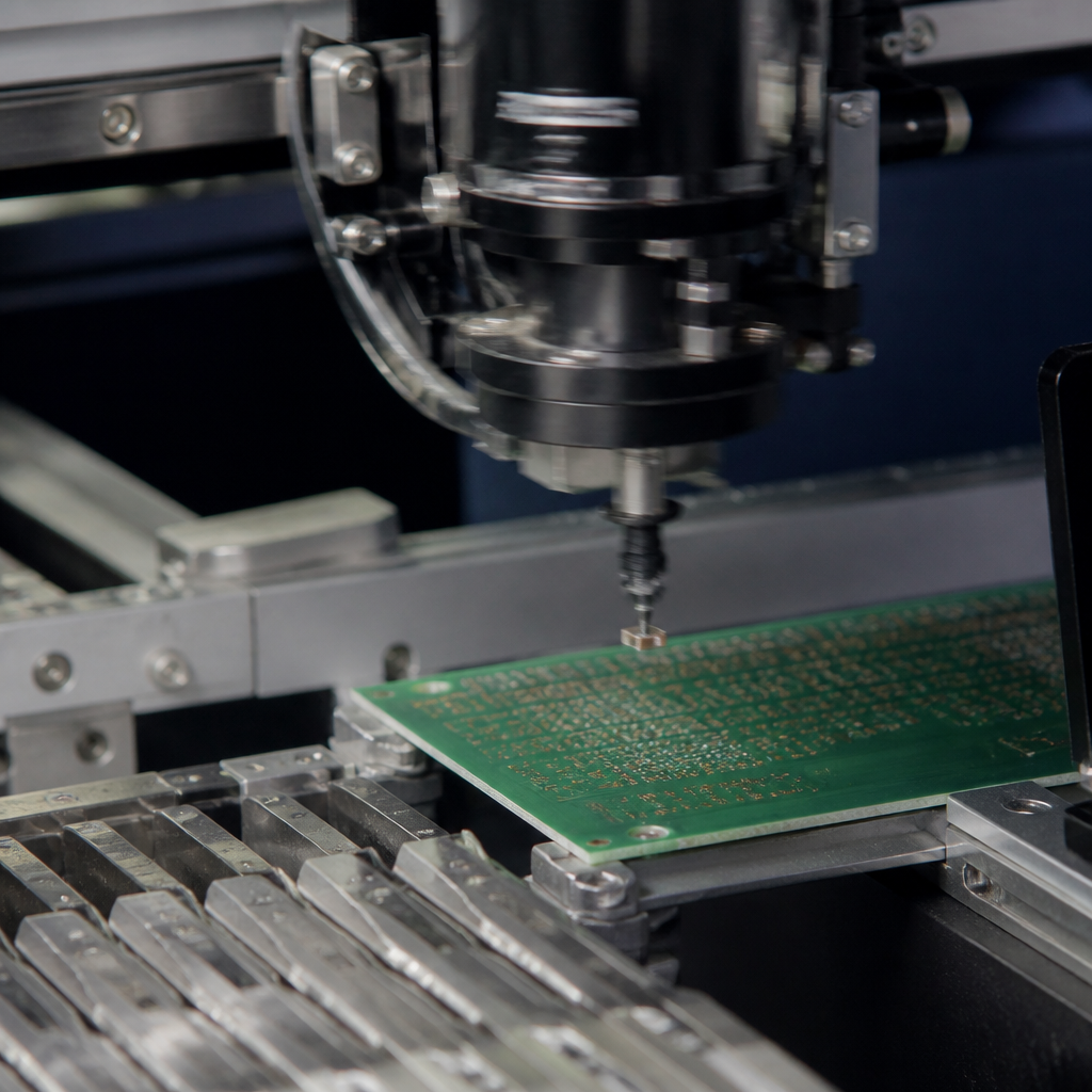
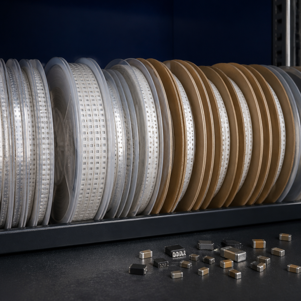
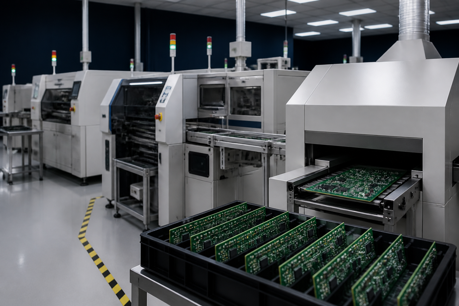
Ten automated SMT lines with high-speed placement machines handle everything from 01005 chips to large BGAs, including mixed-technology THT.
| Placement Speed | Up to 120,000 CPH |
| Min. Component | 01005 (0.4 × 0.2 mm) |
| BGA Pitch | 0.3 mm |
| Board Size | Max 610 × 610 mm |
| Solder Type | Lead-free (SAC305) / leaded |
| Daily Output | 1.5M+ placements |

Our procurement team manages thousands of BOM lines a month through trusted distribution partners — securing genuine parts at competitive prices, even for small batches.
| Min. Order Qty | 1 pc for prototype / low MOQ for volume |
| Lead Time | 1 – 15 days |
| Quality Check | 100% IQC on critical parts |
| Counterfeit Protection | Multi-source verification + X-Ray for high-risk parts |

One contract, one account manager, one invoice. We take full responsibility for your boards from raw material to the shipping dock — you just approve the quote.
| Engineering | DFM / DFA / Gerber check |
| Materials | Full BOM procurement |
| Manufacturing | PCB + SMT + THT + coating |
| Testing | AOI · X-Ray · ICT · FCT |
| Packaging | Vacuum · ESD · export carton |
| Documentation | QC reports · COC · traceability |

Get from idea to first article in days. Our NPI team manages the full journey — quoting, DFM, sample build, validation and ramping to volume without losing momentum.
| PCB Prototype | 24 – 48 hours |
| SMT Sample | 1 – 3 days |
| Small Series | 3 – 7 days |
| Mass Production | 7 – 15 days |

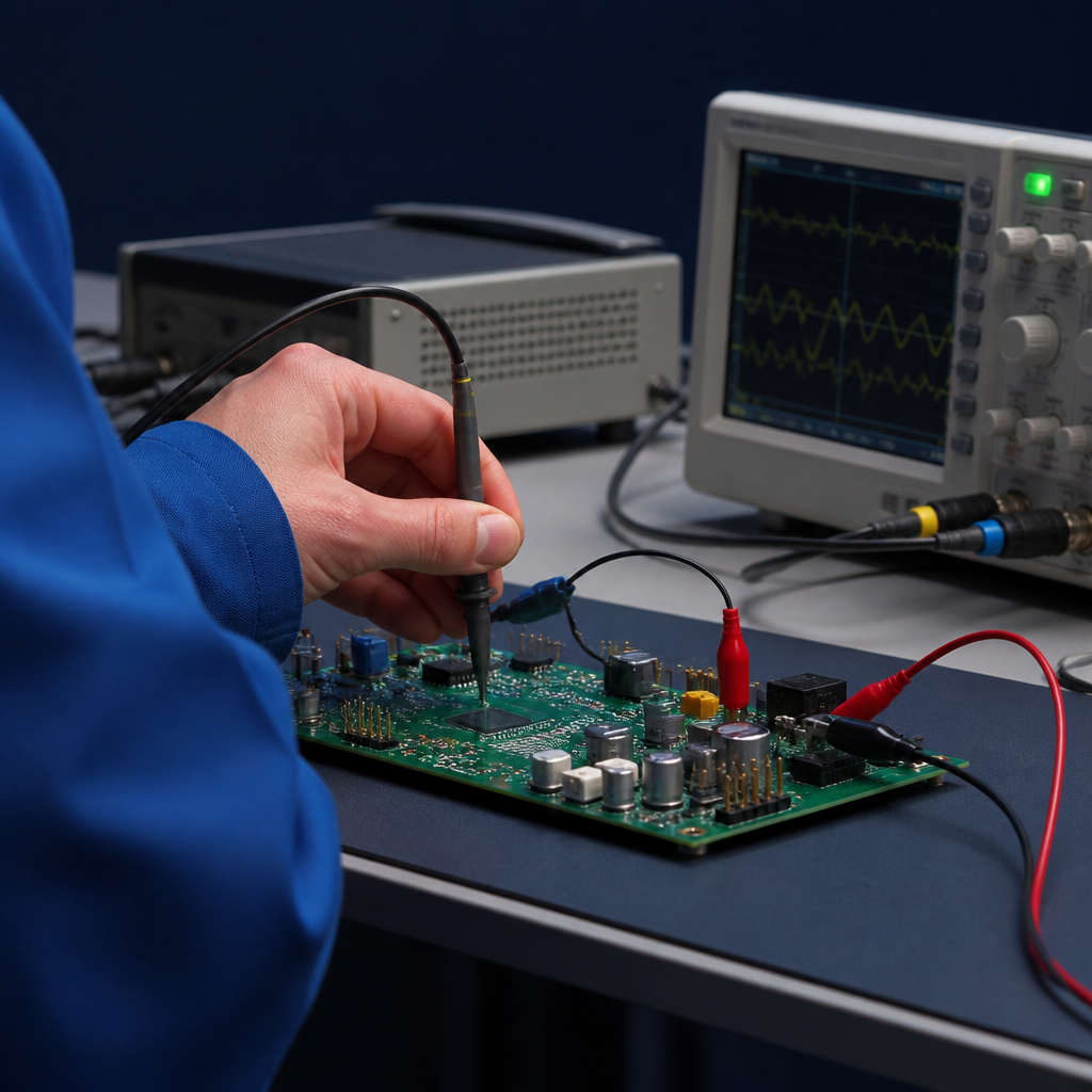
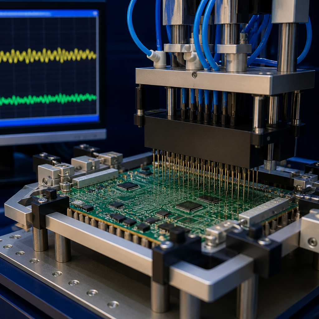
Quality is verified, not assumed. Every assembly passes automated inspection, and we offer full box-build with functional system testing before any shipment.
| SPI | 3D solder-paste inspection on all lines |
| AOI | 100% post-reflow on both sides |
| X-Ray | BGA, QFN and hidden solder joints |
| ICT / FCT | In-circuit & functional testing per spec |
Send your files and let our engineers recommend the most cost-effective path to production.